Researchers at ITMO University have developed a new photoluminescence amplification method for silicon. The metasurface designed by the physicists can enhance silicon's ability to absorb and emit light by 10,000 times – at a record-low volume of the material. The discovery will open the way for faster and more energy-efficient communication devices, as well as nanospectroscopy devices for medicine, science, and industry. The study was published in ACS Photonics.
The silicon light source created by ITMO scientists. Credit: ACS Photonics
Gadgets are prone to heat up from overuse; remember what happens to your smartphone when you watch one too many videos or play games for too long. The problem, nevertheless, can be solved with light particles, photons. In optical systems, photons serve the same function as electrons in devices. However, they release far less heat energy – and additionally facilitate faster logical operations as opposed to electrons.
For a switch to optical computing, electronic devices based on integrated circuits need to be replaced with their optical analogs. The problem is that practically all devices today need silicon to work – this material is used in most elements for data collection, processing, and storage because it is relatively cheap and durable. Silicon has become a backbone of some optical systems; although it has never been deemed popular as a light source. All this is due to its low quantum efficiency – the difference between the number of photons absorbed and the number of photons emitted.
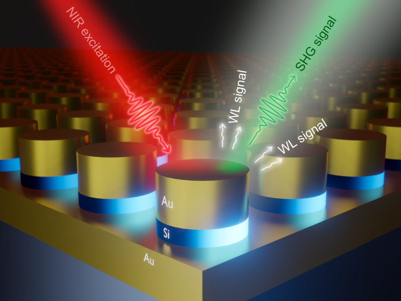
ITMO researchers found a way to increase the material’s quantum efficiency by 10,000 times (from 10-7 to 10-3) by developing a metasurface that “traps” photons and “holds” them in silicon-filled areas. These structures are created using gold lithography. This metal was chosen because it doesn’t actively interact with air, has low absorbance in the visible light range, and is convenient to use in such structures. Gold lithography is performed as follows: a periodic array of gold cylinders is formed on a gold film with gaps between the cylinders and the film; then, these gaps are filled with silicon.
“We use this peculiar geometry to achieve optical resonance. Light of a given wavelength localized within the gaps between the gold film and disks starts to actively interact with silicon. Optical resonances are set up to effectively absorb near-infrared light and stimulate optical transitions in the visible range. And that’s how we get an efficient light source based on silicon. Furthermore, our structure emits broadband white light made up of all the colors of the rainbow and even some near-infrared wavelengths. This feature is vital for optical computers as it allows us to operate several radiation types simultaneously, rather than monochromatic light exclusively," notes Artem Larin, PhD in physics and mathematics, an author of the paper and a researcher at ITMO’s Faculty of Physics.

Artem Larin. Credit: UMNIK grant competition 2023
Another advantage of the developed light source is the record-low volume of active material it requires; the amount of silicon needed to produce light equals the size of a sphere just 50 nm in diameter.
These structures are essential for producing more effective and energy-efficient communication systems, as well as devices for nanospectroscopy and near-field scanning optical microscopy used in medicine, science, and even industry.
The study was conducted by the Hybrid Nanophotonic Systems Group headed by Dmitry Zuev, a senior researcher at ITMO’s Faculty of Physics.
Share it
Последние новости
-
-
ITMO and Joint Institute for Nuclear Research Launch New Master’s Track in Megascience
-
ITMO Researchers Present World’s First AI Model for Supersensitive Optics Design
-
Compact Silicon Chip by ITMO and PKU Revolutionizes Optical Memory
-
ITMO Researchers Discover New Mechanism to Amplify Exciton Current and Accelerate AI Computations