Scientists from ITMO have developed a new method for creating colorful structured semiconductor perovskite films without the risk of defects or contamination. A special nanopattern that imbues perovskites with optical properties is applied with a laser not onto the perovskite film itself but onto a titanium dioxide substrate. The resulting films can be used to change the direction of luminescence. With such nanostructured semiconductors, it’s possible to develop a new type of solar cells and diodes with improved electrophysical characteristics. The study is described in a paper published in Light: Advanced Manufacturing.
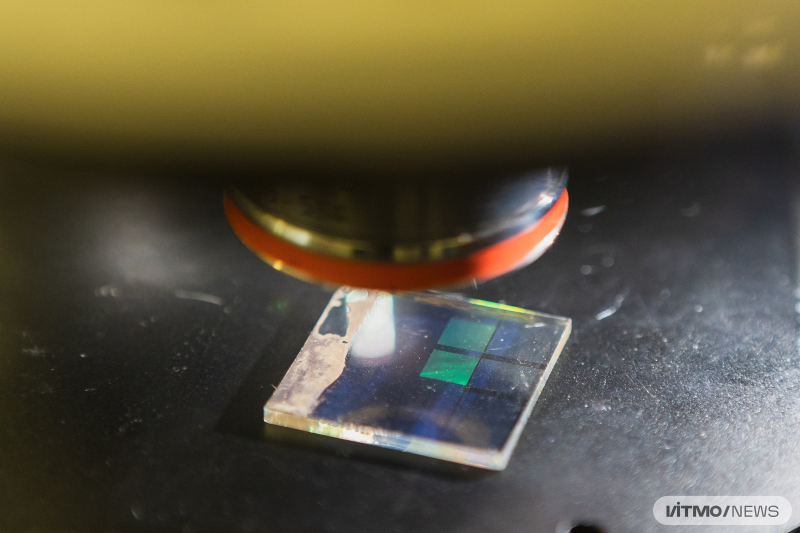
Titanium dioxide films created at ITMO with the laser-induced periodic surface structures (LIPSSs) method. Photo by Dmitry Grigoryev / ITMO NEWS
In recent years, semiconductor perovskites have been increasingly studied as an alternative to silicon in solar cells, photodiodes, and light-emitting diodes. The reason is that they absorb light in the optical range more effectively. Moreover, such semiconductors are easier to produce: they are obtained by solution chemistry methods – a faster and more economical approach suitable for mass production. At the same time, the quality of the raw materials (i.e. the reagents used to synthesize the semiconductors) is less critical for producing efficient device components, as they are less prone to defects.
An important step in producing nanoelectronic devices is often the nanostructuring of semiconductor films. It can, for instance, improve the semiconductor properties of materials or their photoabsorption. One of the most common methods for nanostructuring perovskites is ion beam etching, which involves removing material using an ion beam with electron microscopy equipment. With this method, it’s possible to achieve the desired optical properties in the material. In most cases, a laser interacts directly with the perovskite. However, this usually leads to its ablation – removal from the surface – and charring, which hinders the creation of modern multilayer devices such as solar cells and light-emitting diodes.
Physicists at ITMO have suggested a method that involves “etching” the nanopattern onto perovskites without directly impacting them with a laser. With the laser-induced periodic surface structures (LIPSSs) method, it’s possible to form the nanopattern not on the film itself, but on a titanium dioxide film subjected to a pulse laser in a specific mode. The laser’s light is absorbed by the film, which causes a surface plasmon resonance – this is when the frequency of incident light matches the frequency of synchronous oscillations of electrons on the film’s surface. This causes the film to locally melt and then instantly set again, forming grooves of various shapes and sizes in the surface of titanium dioxide. After that, the titanium dioxide film is applied onto the perovskite film, which acquires its properties.
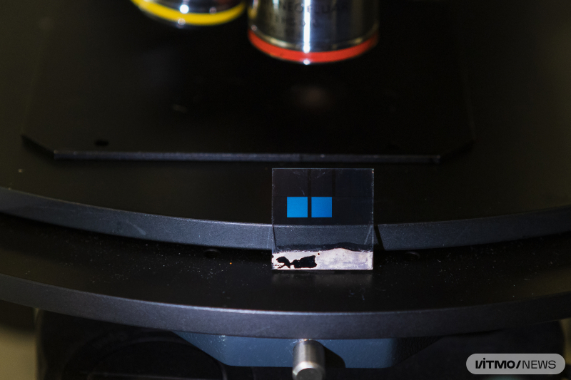
Titanium dioxide films created at ITMO with the laser-induced periodic surface structures (LIPSSs) methods. Photo by Dmitry Grigoryev / ITMO NEWS
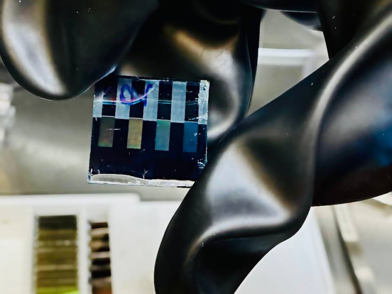
Perovskite films created at ITMO with the laser-induced periodic surface structures (LIPSSs) methods. Photo by Dmitry Grigoryev / ITMO NEWS
The resulting nanopattern resembles ripples on the surface of the sea or sand dunes – it repeats with a certain periodicity. This period determines the diffraction properties of the perovskite film, that is, the colors we see on its surface: shades ranging from green to blue. Originally, the perovskite is brown in color, but when light localizes in the “grooves” of the nanopattern, it refracts at a different angle and takes on a different color. This optical effect precisely replicates the natural mechanism of color formation on butterfly wings: their small scales localize and refract light at specific angles, resulting in a color change.
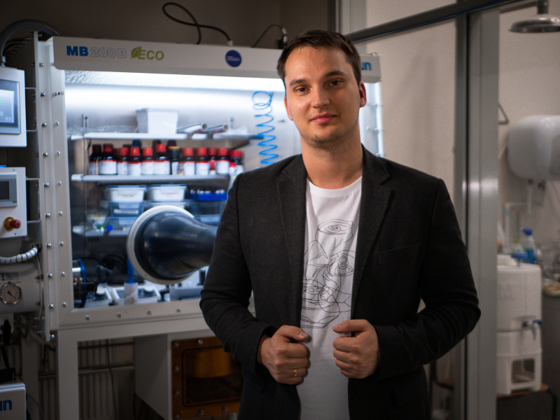
“We discovered that the nanopattern also determines the photoluminescent properties of perovskite films, in particular the photoluminescence directionality diagram – the so-called cold radiation. In other words, we can “direct” the light into the necessary field. As we rotate the film at different angles, the luminescence will increase or decrease, meaning that we’ll get a brighter or dimmer lighting source without changing any other properties of the material. This proves the anisotropy of light, which is the key result of our study,” says the paper’s first author Dr. Alexandra Furasova, a senior researcher at the Laboratory of Hybrid Nanophotonics and Optoelectronics of ITMO’s Faculty of Physics.

Alexandra Furasova. Photo by Dmitry Grigoryev / ITMO NEWS
Another advantage of the new method is the high “writing” speed of the nanopattern onto the film. In just a minute, it’s possible to create up to 1 cm2 of a nanopattern on titanium dioxide. And as physicists work with nanoscale objects, the time will be even shorter. Moreover, titanium dioxide films can be reused: the perovskite films can be washed off and replaced with new ones. The films’ size is also variable. Thanks to these properties, such semiconductors have scaling potential.
“Importantly, in our work we used cutting-edge laser technologies for fast, high-quality writing of coloring nanostructures. Together with our colleagues from ITMO’s Institute of Laser Technologies, we were able to optimize the process to the point that we were able to use industrial laser systems for precision tasks – when the modified titanium dioxide film is 1,000 times thinner than a human hair,” adds Prof. Sergey Makarov, the chief research associate and head of the Laboratory of Hybrid Nanophotonics and Optoelectronics of ITMO’s Faculty of Physics.
Sergey Makarov. Photo by Dmitry Grigoryev / ITMO NEWS
In the future, the developed perovskite films can be used to create a new type of high-efficiency solar cells, diodes, and photodetectors. The team is already working on the next step of their project: testing the films in real-world devices.
This study was supported by a Russian Science Foundation grant and the national program Priority 2030.
Share it
Последние новости
-
-
ITMO Scientists Create World’s First Wirelessly Chargeable AA Battery
-
ITMO and Joint Institute for Nuclear Research Launch New Master’s Track in Megascience
-
ITMO Researchers Present World’s First AI Model for Supersensitive Optics Design
-
Compact Silicon Chip by ITMO and PKU Revolutionizes Optical Memory