


Researchers from ITMO University, Skoltech, and HSE University have developed the first electrically powered perovskite laser that requires no additional external lighting from another laser or a powerful lamp; instead, it can be directly connected to a power source like a regular LED. Since perovskite crystals can be easily grown from solutions, the technology is more cost-efficient than existing alternatives – and can potentially be used in optical chips, sensors, and quantum devices. The findings of the corresponding study were published in Nature.
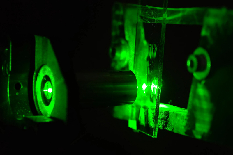
Credit: Ludya / photogenica.ru
For lasers to produce directional light, their active medium, commonly a semiconductor crystal, must be supplied with energy from an external source. This is usually done using another laser or a powerful flash lamp. However, an additional power source makes the resulting setup rather bulky.
To eliminate external sources and make lasers small enough to fit directly on a chip, scientists have long aimed for electrical pumping. One of the most promising materials for feeding current directly into a device, as in regular LEDs, are artificial crystals called perovskites, which can efficiently convert electrical energy into light. That said, building such a laser is not easy; one of the reasons being that when exposed to an electric current and metal electrodes, perovskite crystals deteriorate rapidly as they exhibit poor thermal stability and are prone to overheating.
In solving the problem of overheating and destruction, the team of scientists from ITMO University, Skoltech, and HSE University abandoned metal electrodes in favor of single-walled carbon nanotubes – the material, which does not destroy a perovskite when current passes through the crystal. The active medium of the laser, namely a perovskite microplate, was grown out of a chemical solution via controlled crystallization in which a structure forms gradually, as the liquid evaporates. This approach is much simpler and cheaper compared to layer-by-layer material deposition in vacuum chambers, which is common in manufacturing such devices.
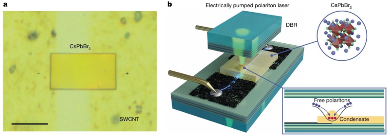
Architecture of the perovskite polariton laser diode: CsPbBr3 – the chemical formula for the perovskite material and a raised area on its surface (pic. b) – the site of a physical defect that enables trapped polariton condensation and radiation generation. Illustration by Anatoly Pushkarev and other researchers / Nature
The scientists placed the solution-grown crystal between two distributed Bragg reflectors; the reflectors trap light inside and reflect it back and forth, so that it amplifies on the output. With this setup, they were able to implement a principle that is fundamentally different from that of conventional lasers. Between two parallel mirrors the light repeatedly reflects and is trapped within a limited space where it interacts with the perovskite. Then, a series of transformations occurs: the light converts into crystal electron excitations and back, causing polaritons, i.e. particles, which are part light and part matter, to appear. In their turn, low-mass polaritons begin to interact with one another, making the transition to a Bose-Einstein condensate possible. In this state of matter, multiple polaritons start to behave as a single whole – this exact principle underpins polariton-based lasers.
The experiments demonstrated the polariton lasing with a threshold of 60 μA under continuous electrical injection. Prior to this, direct electrical pumping of a perovskite laser remained an unresolved challenge.
Since such crystals are solution-grown and need no complex and expensive equipment, they can potentially make mass production of devices based on them easier and cheaper.
For now, the device can only operate in a cooling chamber where the temperature does not exceed -265 °C, which severely restricts its practical use. In the long run, the researchers expect to achieve stable operation at room temperature; for that, they will need to improve heat removal from the crystal and enhance material stability to prevent degradation during long-term operation. If the team succeeds, the next-gen lasers can be integrated onto microchips and employed in portable electronic devices.
Furthermore, the scientists plan to move from a single emitting element to entire arrays – sets of multiple lasers interacting with one another – to produce more complex optical systems, with light flexibly controlled right on-chip.

Alexey Yulin. Photo by Dmitry Grigoryev / ITMO NEWS
“Polariton systems present an interesting case for nonlinear optics because light can trigger rapid and drastic changes in their crystal properties – much stronger than, for example, in silicon. This allows us to observe unusual phenomena, including the formation of polariton condensates, the transition of numerous polaritons into the ground quantum state. In this context, perovskites serve as one of the most promising platforms due to the potential simplicity of production and high light-generation efficiency. In our recent research, we were the first to demonstrate that electrically pumped lasing was possible in such systems,” explains Alexey Yulin, a leading researcher at ITMO’s Faculty of Physics responsible for the theoretical support and modeling of the technology.
The study was supported by a Russian Science Foundation grant led by Alexey Yulin. The collaboration was possible due to long-standing ties between the institutions: many researchers from ITMO University, Skoltech, and HSE University have previously collaborated on other projects, including the joint program Clover. Three researchers from ITMO's Faculty of Physics – the laboratory assistant Alexey Ekgardt and PhD students Daria Khmelevskaia and Alexandr Marunchenko – took part in the study.
Share it


Последние новости
-
-
ITMO Scientists Devise Way to Apply Hybrid Light Particles in Ultrafast Optical Chips
-
ITMO Scientists First to Describe Full Photon Lifecycle in Time and Space
-
ITMO Scientists Develop New Ultrasensitive Sensor Design for Medical Diagnostics That Outperforms Counterparts
-
Light From Nowhere: ITMO Scientists Explain How Twisted Electrons Emit Photons Outside Magnetic Fields