Researchers from ITMO University and the Pohang University of Science and Technology (POSTECH) in South Korea have merged a metasurface and a 2D semiconductor to produce a next-gen light-emitting element that is 1,600 times brighter than a semiconductor surface and even more durable and thinner than same-brightness analogs. The new material will pave the way for ultra-thin screens and other optical devices. The resulting paper was in Light: Science & Applications.
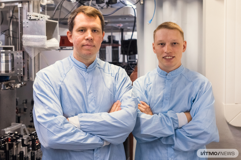
Vasily Kravtsov and Artem Abramov, a PhD student at ITMO and a co-author of the paper. Photo by Dmitry Grigoryev / ITMO NEWS
The most common light sources for AR glasses, ultra-thin screens for PCs, smartphones, and automobiles, as well as other optical devices, are light-emitting transparent components, typically organic light-emitting diodes (OLEDs). However, these materials have low transparency and tend to lose integrity and brightness over time. Today, physicists are working to reduce the thickness of light-emitting components in order to improve their transparency. One promising material for such elements are 2D crystalline semiconductors, which not only radiate more light, but are also more durable than their organic analogs. The problem is that their quantum efficiency is less than 1%, which is 100 times less than required for its practical use.
To increase the radiation area and efficiency of the material, ITMO researchers and their colleagues from POSTECH have combined a MoSe2 monolayer and a plasmonic gold metasurface. The latter is an array of slot nanoantennas that support two types of optical resonances – they reinforce one another and increase radiation in a 2D semiconductor layer. For that reason, the resulting material exhibits a 1,600 times higher brightness when compared to a conventional semiconductor monolayer, which is not coupled with a metasurface. When a one-micron laser reached the component, it emitted roughly 800 µm2, or about 25-30 µ, which is the size of one pixel on a modern TV.
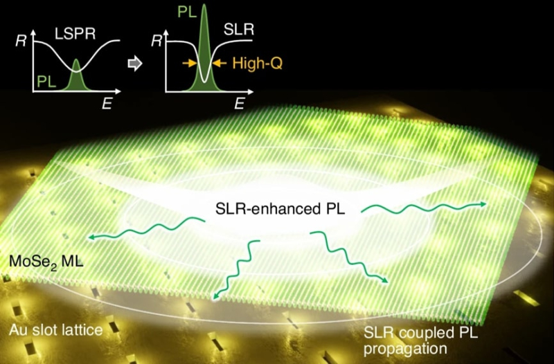
An optical emission enhanced through the interaction of a single-layer semiconductor with resonances of a gold metasurface. Credit: Light: Science & Applications
The material is ultra-thin; its active layer is measured at 0.7 nm, and the entire structure is at about 30 nm – but these parameters can be decreased further, the physicists claim. The element endures negative effects of light and electricity due to its crystal structure. It is expected to have practically no lifespan limit, whereas that of organic light-emitting elements is about two years.
“So far, we used laser radiation on our samples, but we want to achieve radiation that will be triggered by an electrical pulse. For that, we’re building a device that will be connected to our structure through electrical contacts so that we can run tests on optoelectronic devices. Then, we also want to increase the number of semiconductor layers and assemble a heterostructure. Such light-emitting components have an increased lifetime of excited states and new degrees of freedom for optical states to be stored in. Potentially, this will bring us closer to creating compact devices that can simultaneously detect, process, and transmit optical data,” says Vasily Kravtsov, an author of the paper and a senior researcher at ITMO’s Faculty of Physics.
The project is supported by the national program Priority 2030.
Elizaveta Kokorina
Journalist
Marina Belyaeva
Translator